

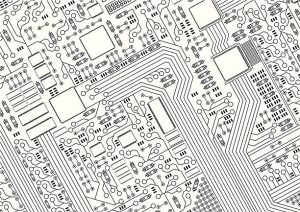
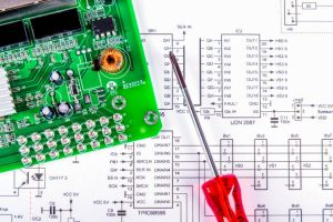
With the increasing complexity and expanding functions of electronic devices, PCB layout online becomes more and more critical in the whole electronic design process. Nowadays, with the development of Internet technology, more and more PCB design work can be completed through online tools, this trend not only enhances the flexibility and convenience of design but also gives rise to new opportunities for technological innovation. In this paper, the importance and potential of online PCB layout tools in terms of innovation and future development will be discussed in depth.
AI and PCB Layout Online
Artificial Intelligence (AI) as a key technology is profoundly affecting the way PCB layout online is done. While traditional PCB layout relies on engineers’ experience and rules, AI technology enables automated layout design through big data analysis and algorithmic optimization. Specifically:
- Intelligent wiring technology: AI can optimize signal transmission paths, reduce signal interference, and improve board performance stability and reliability. According to Mentor Graphics research, the use of AI to optimize the layout can reduce the signal transmission time delay by an average of 20%, significantly improving the efficiency of the circuit board.
- Design optimization algorithms: AI algorithms can analyze a large number of design rules and component layout data to find the best design solution. For example, Cadence’s Allegro tool integrates AI-driven design optimization to help designers ensure performance while effectively reducing cost and time investment.
- Example analysis: Altium Designer, for example, its AI-assisted design tools can automatically adjust the location of components according to the circuit board layout requirements, optimize the wiring path, and reduce manual intervention. This intelligent design not only improves design efficiency but also reduces the risk of design errors, effectively shortening the time to market.
Applications of VR and AR
With the development of virtual reality (VR) and augmented reality (AR) technology, their application in PCB design is gradually showing great potential, let see how PCB layout online works:
- Virtual prototype: Virtual Reality technology can transform the PCB design into a real three-dimensional model, the designer can intuitively view and modify the design through the virtual environment, this is more intuitive and operational than the traditional graphic design.
- AR-assisted layout: Augmented reality technology can provide real-time feedback and guidance in the actual work, designers can see the location of virtual components and wiring paths in the real world through AR glasses or mobile phone applications, making the PCB layout online process more efficient and accurate.
- Industry Practice: According to market research, more than 40% of PCB design teams are considering or already using augmented reality technologies to improve their design process. These technologies not only improve designer productivity but also accelerate product innovation and development cycles.
Conclusion:
In the future, PCB layout online tools will continue to influence and change the way electronic designers work. Through cloud-based technologies and online platforms, design teams can achieve global collaboration, regardless of geographical and time zone restrictions, and improve teamwork efficiency and responsiveness.
It also helps to reduce the consumption of physical resources by reducing the need for traditional raw materials through digital design and virtual prototyping, thus contributing to environmental sustainability. Thus the potential for PCB layout online is unlimited.